NSL Facilities
NanoSystems Laboratory The Ohio State University        Help Buckeye link Map Find people Webmail
menu divider
Nanosystems Laboratory Banner
Click Grayed area to get more details.

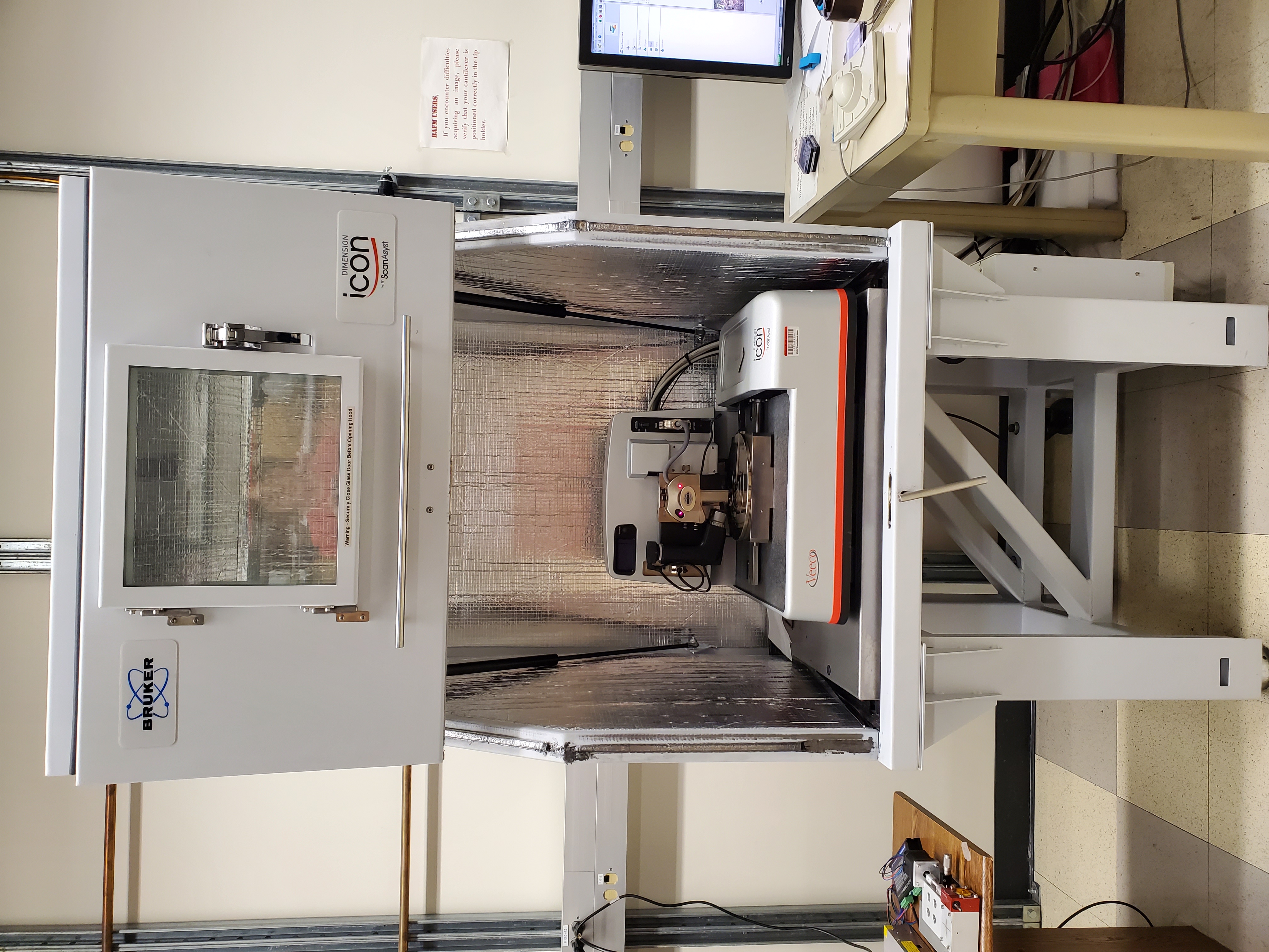
Bruker AXS Dimension Icon Atomic/Magnetic Force Microscope with ScanAsyst

Located in PRB 1159

  1. Vibration isolation and sound proof enclosure for low noise operation
  2. Closed loop scanner with scan range 90 µm x 90 µm
  3. Z sensor noise level (closed-loop) of 35 pm RMS typical in imaging bandwidth of 625 Hz
  4. Easy sample positioning with 5-megapixel digital camera with digital zoom and motorized focus
 

Bruker Atomic Force Microscope
Modes of operation include:
  1. Atomic Force Microscopy (AFM) mode
  2. Magnetic Force Microscopy (MFM) mode
  3. PeakForce Quantitative Nanomechanical Property Mapping (PF-QNM) mode
  4. Scanned Capacitance Microscopy (SCM) mode
  5. Spatially resolved electrical characterization mode
Bruker Atomic Force Microscope

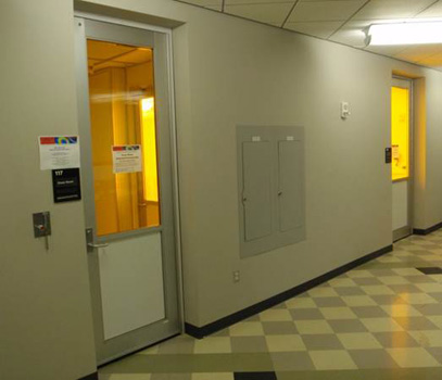
Clean Room

Located in PRB 0115/0117

  1. 1,100 ft2 clean room space
  2. Class: 1000
  3. Instruments house here include the Lab-18 Sputtering System, Laurell Spinner
Clean Room

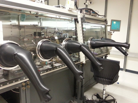
Organic Clean Room

Located in PRB 2185

1,100 ft2 of class 10,000 clean room space optimized for chemistry of air sensitive organic materials.
The clean room features four interconnected glove boxes with nitrogen or argon atmosphere available. The glove boxes contain two thin film PVD chambers with the following two capabilities.
  1. The metal film deposition chamber is equipped with one e-beam, one sputter, and two thermal evaporation sources.
  2. The organic film deposition chamber is equipped with two OLED and two thermal evaporation sources.
  3. The clean room also features a yellow room for substrate preparation, with a fume hood, an ultrasonic cleaner, a UV ozone cleaner, and an optical microscope.
Organic Clean Room

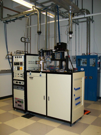
Diamond Chemical Vapor Deposition Stystem (CVD)

Located in PRB 1119

  1. State-of-the-art deposition tool for synthesizing high quality poly crystalline and single crystal diamond films for research and production
  2. The system is available with process gases: H2, CH4, O2 and N2
  3. Substrate heating up to 900°C
  4. Capability for biased substrate nucleation growth
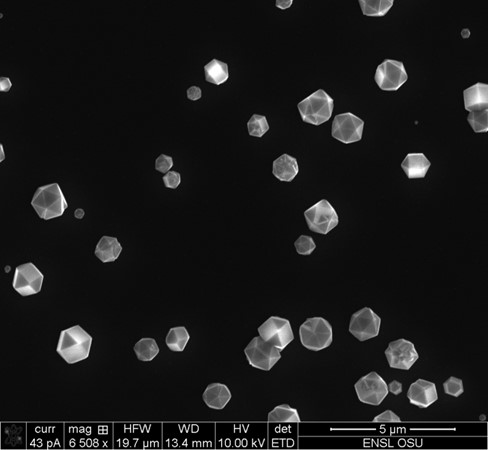
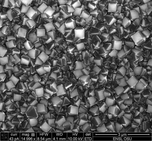
Polycrystalline diamond growth:
CVD1 CVD2
SEM images of polycrystalline diamond films grown at different substrate biases demonstrating control over nucleation process by controlling bias voltage. Dr. C. Marginean
CVD

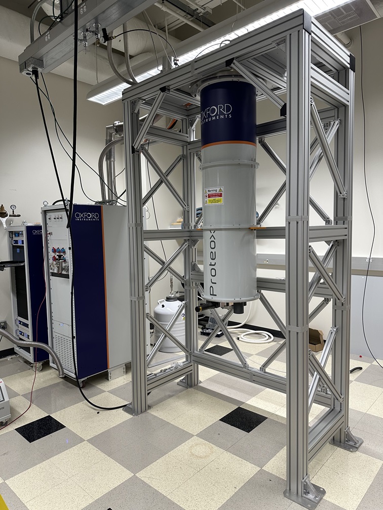
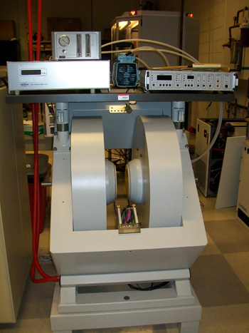
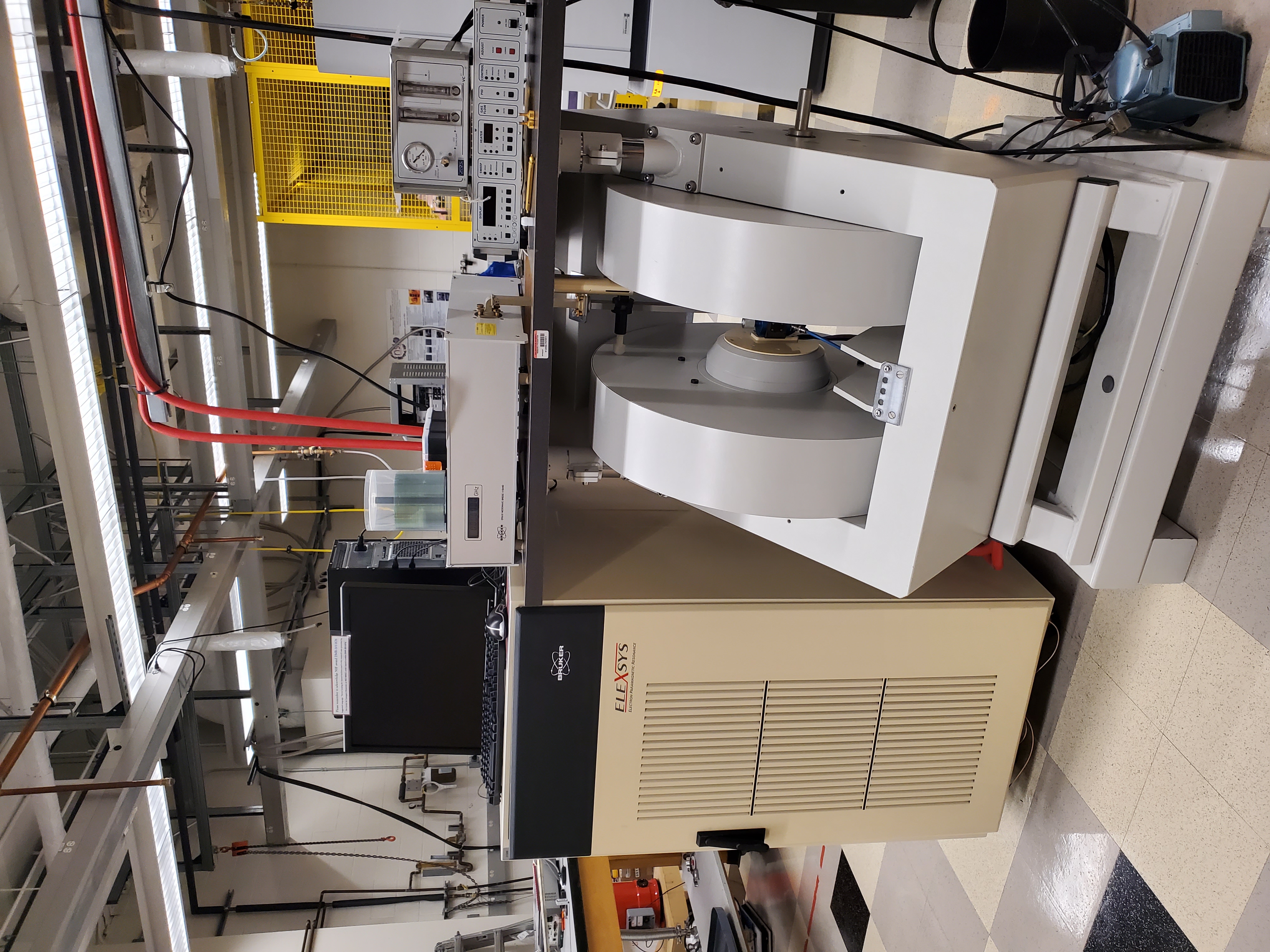
Electron Paramagnetic Resonance Spectrometer (EPR)

Located in the PRB 0177

  1.   a
  2.   b
  3.   c
  4.   d
Electron Paramagnetic Resonance Spectrometer 

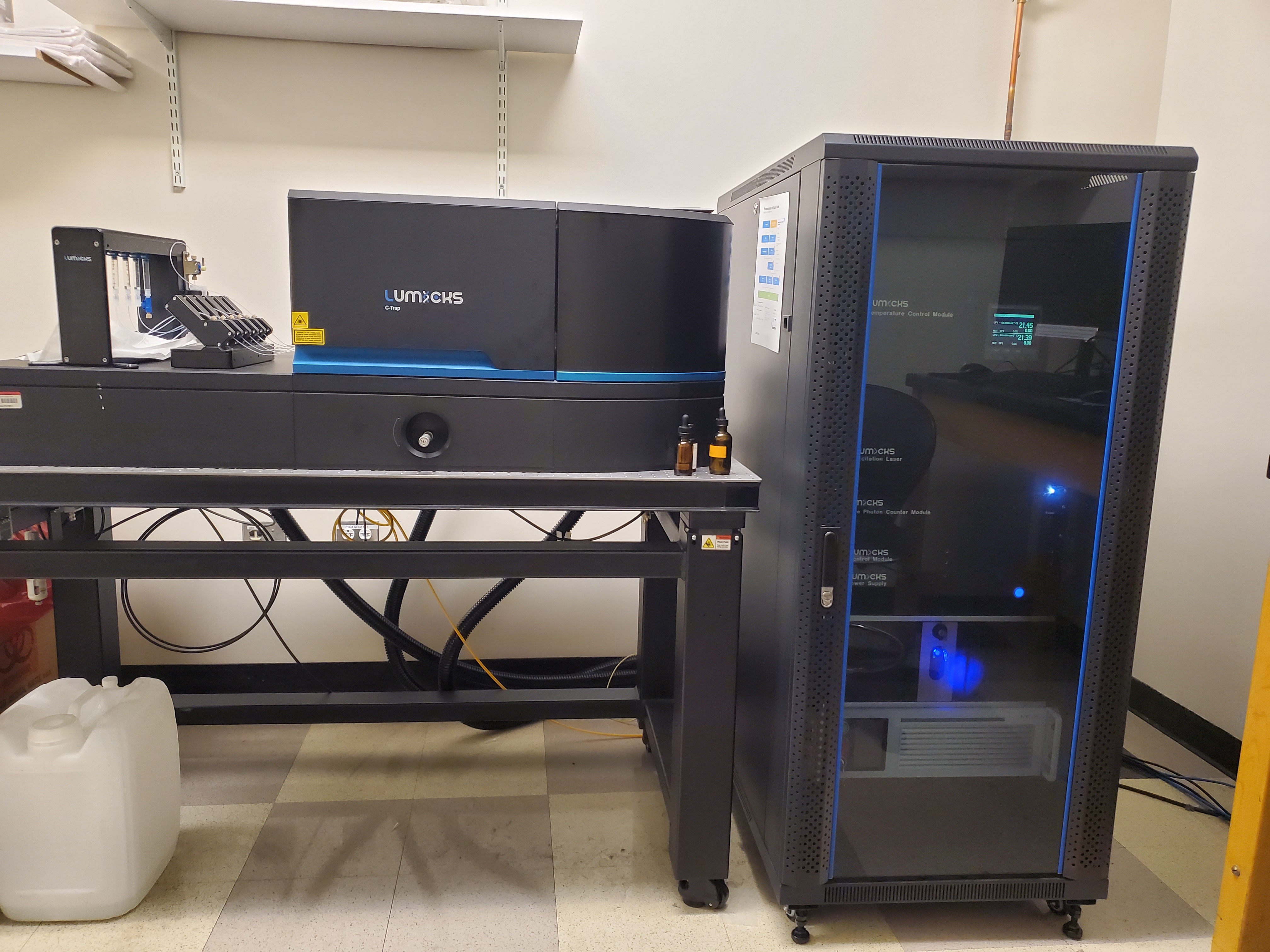
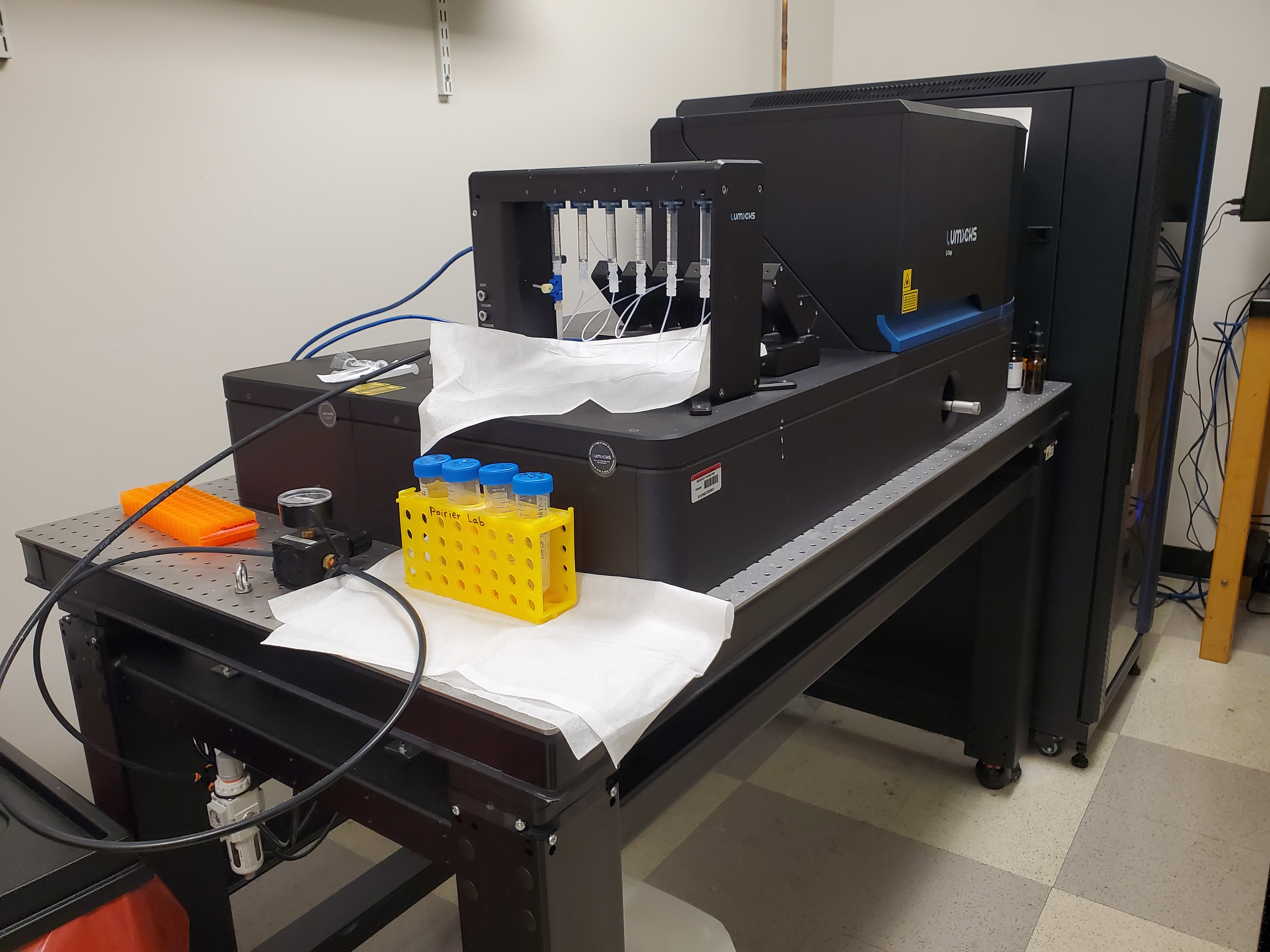
C-Trap® Optical Tweezers – Fluorescence & Label-free Microscope by LUMICKS (Amsterdam The Netherlands)

Located in the PRB 0136

  • C-Trap® uses two laser beams traveling through a microscope objective to create two highly focused beams of light strong enough to trap and hold in place or move objects such as plastic beads traveling in a microfluidic channel. These beads can be coated to stick to a variety of biomolecules, such as proteins, cytoskeleton filaments, DNA, or RNA. Furthermore, the tiniest forces applied to these molecules can be measured as well, creating a tool not only capable of manipulating biomolecules but also capable of detecting what’s happening to them.
  • C-Trap® also includes a capability for the multicolor confocal fluorescence imaging that allows the visualization of biological processes such as protein kinetics and (un)binding events on DNA.
C Trap1 C Trap2
Mechanisms are at the heart of understanding biology
Currently available methods provide incomplete insight into biological mechanisms
Our solution: the C-Trap
Multi-user system with a range of different applications
Images provided by LUMICKS.

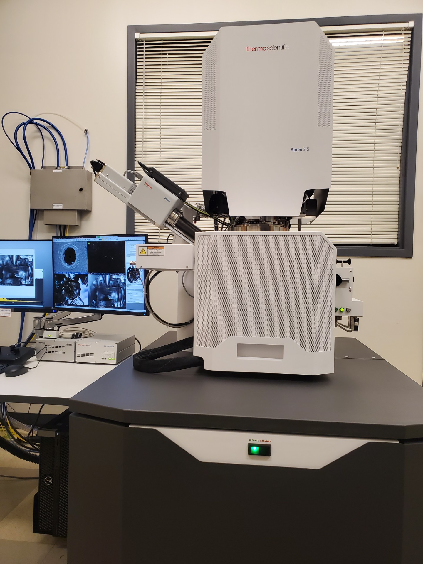
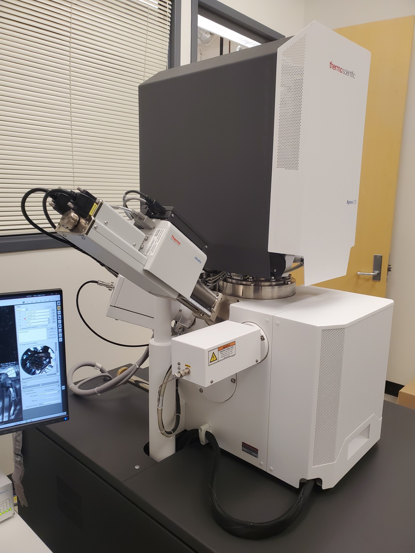
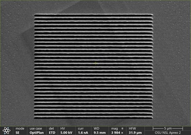
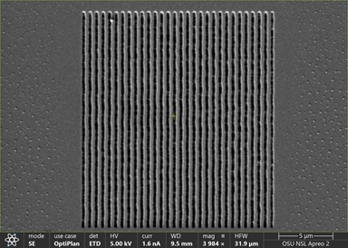
Thermo Fisher Scientific Apreo 2S ChemiSEM Scanning Electron Microscope

Located in PRB 0177C

  • Apreo 2S is a field emission gun (FEG) SEM with high performance, resolution, and contrast that combines advanced optics and detection with automation thus making obtaining high resolution imaging possible even for users new to SEM.
  • Imaging resolution of 1.0 nm - 0.8 nm is achievable depending on the sample material, applied voltage (500 V - 30 kV) and working distance.
  • Live quantitative SEM image coloring with ChemiSEM Technology is available based on energy dispersive X-ray spectroscopy (EDS). Point & ID, linescan, region, element maps are included.
  • Low vacuum mode is available for imaging dielectrics with achievable 10 – 50 Pa water vapor chamber pressure.
  • Multi-purpose sample holder is available. It hosts up to 18 standard stubs (Ø12 mm), three pre-tilted stubs, two pre-tilted row-bar holders (38° and 90°), a Faraday cup and does not require tools to mount a sample
  • Electron channelling contrast imaging (ECCI) mode is available. ECCI is an electron diffraction technique enabling the study of defects in materials including dislocations or stacking faults that are close to the surface of the sample, low angle grain boundaries or atomic steps.
  • CleanConnect Sample Transfer System, available on the instrument, enables quick sample transfer without exposing air-sensitive samples to atmosphere by maintaining inert gas or vacuum sample environment.
  • The SEM is equipped with Nanometer Pattern Generation System (NPGS) v9.2 which is an SEM e-beal lithography system. NPGS uses QCAD, which is an open source CAD system, for pattern design.

Scanning Electron Microscope Apreo 2S ThermoFisher Scientific Apreo 2S

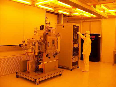
Kurt J. Lesker Co. Lab 18 Thin Film Deposition System

Located in the NSL cleanroom, PRB 0115/0117

  • Three 3” sputtering sources and one 6-pocket e-beam evaporator in the same deposition chamber
  • RF and DC sputtering capabilities
  • Two process gases: Argon and Oxygen
  • Substrate cleaning with RF plasma
  • Optimized for sputter deposition of magnetic metals and/or oxides followed by coating with a precious metal (gold, platinum) using e-beam deposition
  • Rapid turn-around operation with a load lock
  • Aggressive substrate cleaning and sample ion milling with a collimated Kauffman & Robinson KDC-40 ion source installed in the load lock
  • Installed in clean room environment


Available sputter targets:

  • Aluminum (Al)
  • Cobalt (Co)
  • Cobalt/Iron (Co/Fe)
  • Copper (Cu)
  • Copper/Nickel (Cu/Ni)
  • Iron (Fe)
  • Niobium (Nb)
  • Nickel (Ni)
  • Nickel/Iron (Ni/Fe)
  • Silicon Dioxide ( SiO2 )
  • Tin (Sn)
  • Tungsten (W)

Available e-beam materials:

  • Aluminum (Al)
  • Chromium (Cr)
  • Cobalt (Co)
  • Germanium (Ge)
  • Gold-Germanium (AuGe)
  • Gold (Au) - $0.50/nm
  • Iron (Fe)
  • Magnesium-Oxide (MgO)
  • Nickel (Ni)
  • Palladium (Pd)
  • Permalloy (Py)
  • Platinum (Pt) - $0.65/nm
  • Silver (Ag)
  • Tantalum (Ta)
  • Titanium (Ti)
 
lab 18

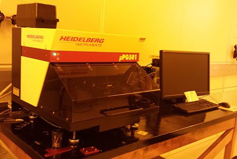
Heidelberg Instruments Tabletop Maskless Aligner System µPG501

Located in the NSL clean room (PRB 0115/0117)

  • Photo lithography for prototyping without a need for a contact mask
  • Computer generated pattern
  • Smallest feature size 1 µm
  • Substrates up to 6” x 6”
  • Address grid 50 nm x 50 nm
  • Easy use with auto focus system
  • Camera system for metrology and alignment
  • High power 390 nm LED
  • Can be used for contact mask fabrication
maskless aligner

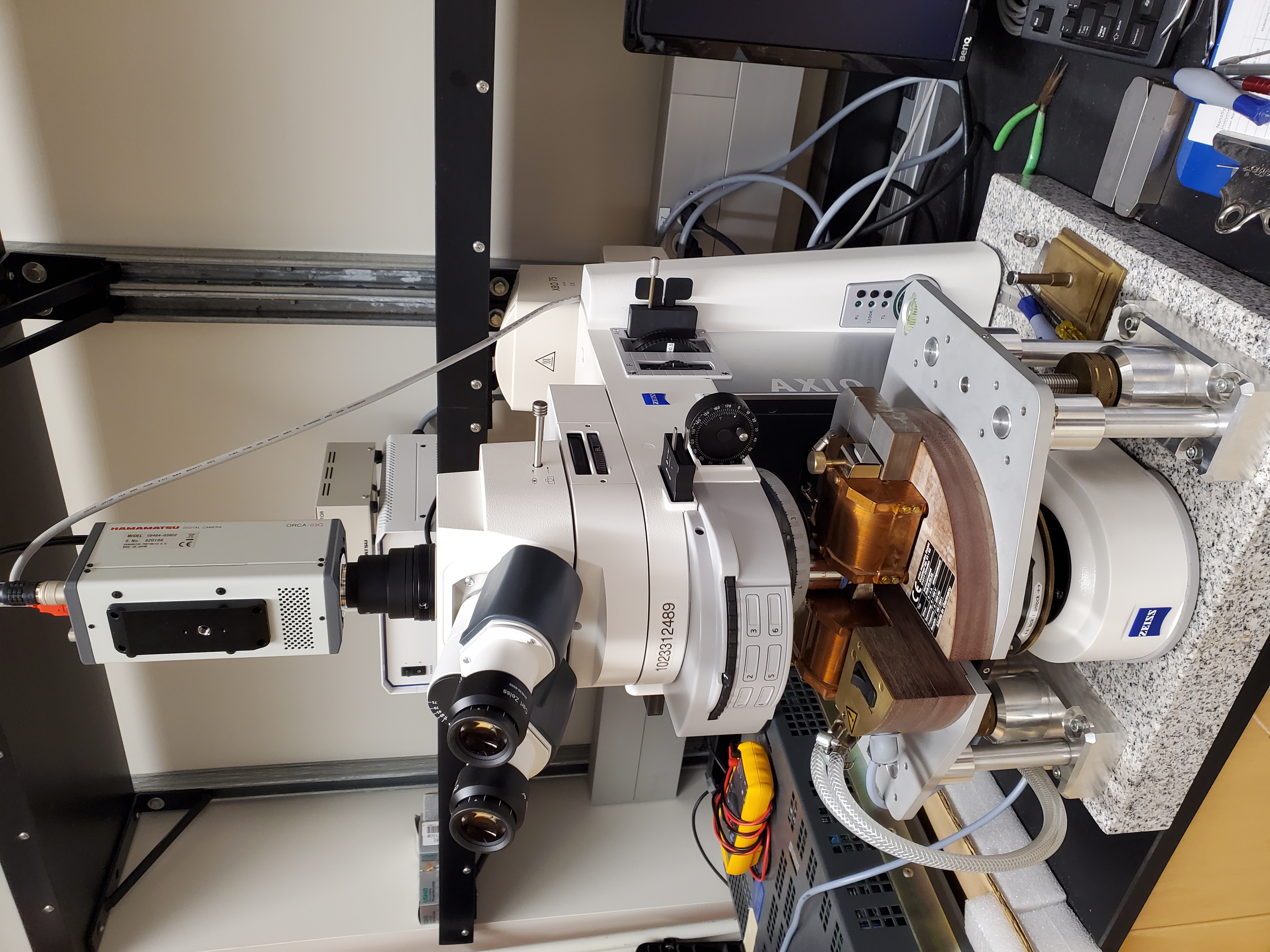
Magneto-Optical Kerr Effect Microscope (MOKE)

Located in PRB 1159

  • a
  • b
  • c
  • d
Magneto-Optical Kerr Effect Microscope

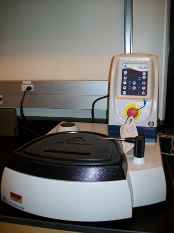
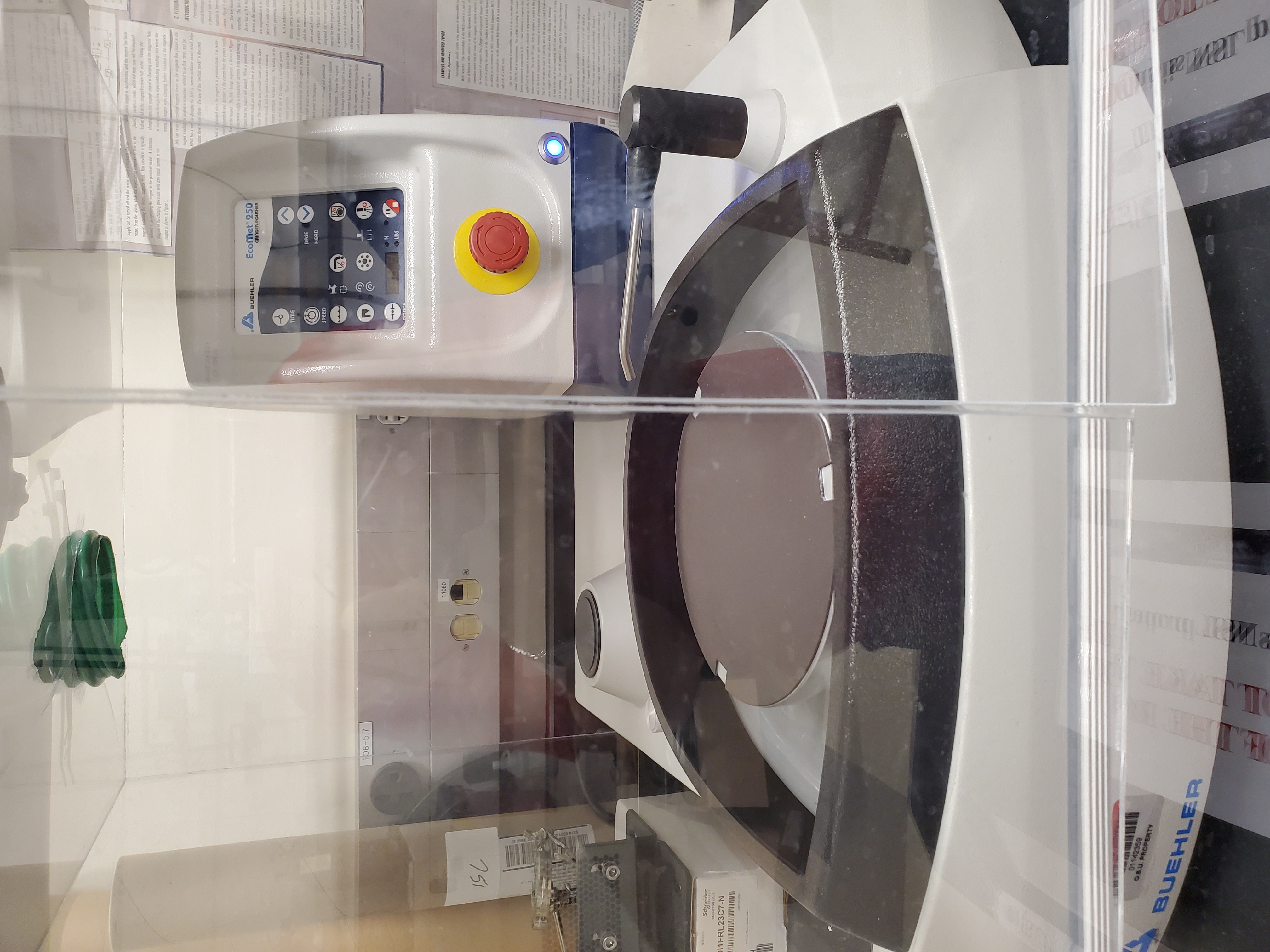
Polisher/Grinder

Located in the Photo Lab, PRB 1119

  • a
  • b
  • c
  • d
Polisher/Grinder 

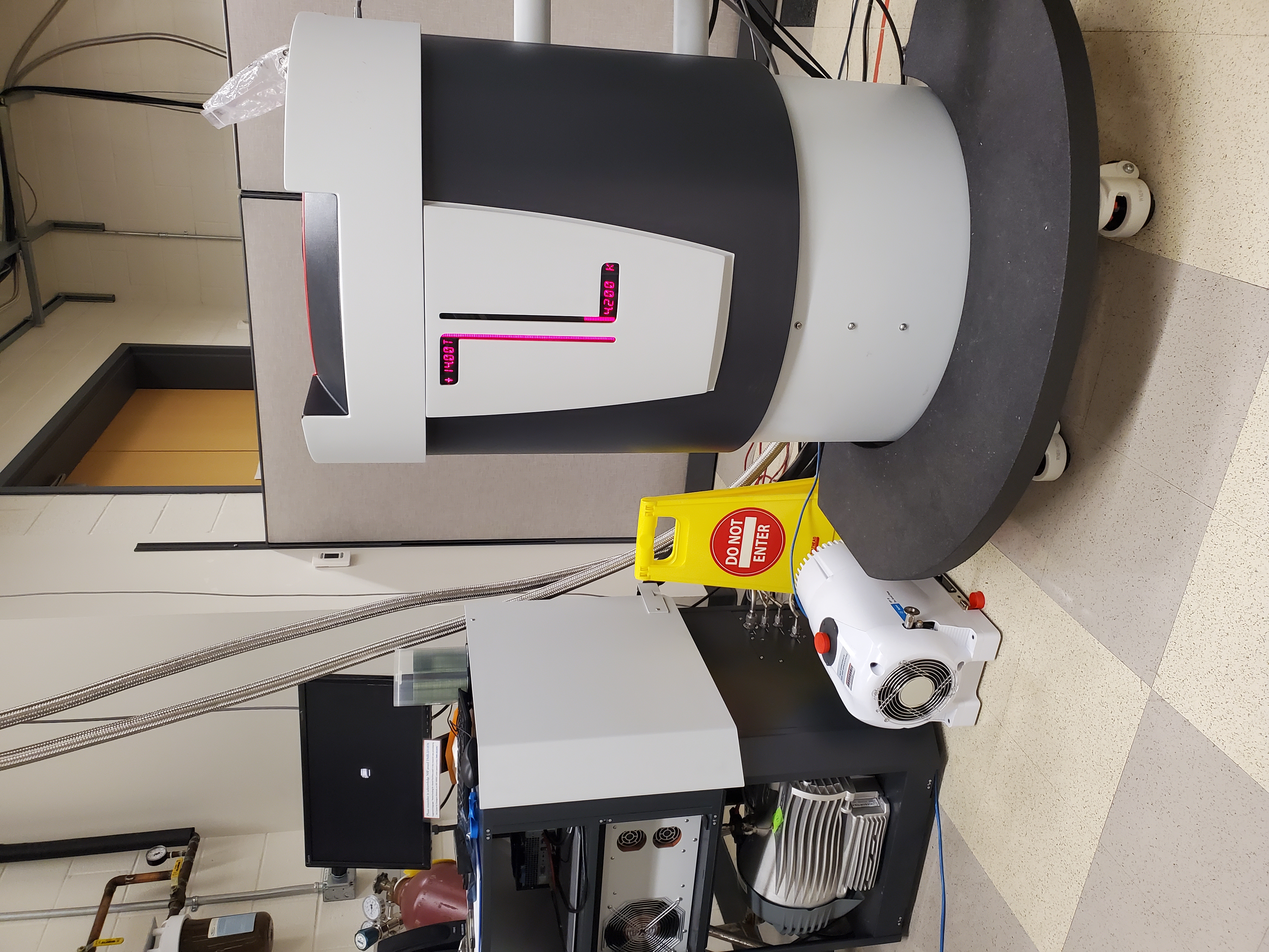
Quantum Design 14 T Physical Properties Measurement System (PPMS) with cryogenic AFM/MFM

Located in PRB 0177

MAGNET ONLY AVAILABLE WITH 14T PROPERTIES
  • Capable of conducting resistivity, AC transport (ACT), AC magnetic susceptibility (ACMS), Vibrating Sample Magnetometry(VSM) and torque magnetometery measurements
  • VSM capability comes with both large and small bore coil sets and a high temperature oven option with the capability for sample heating up to 1100 K
  • Measurements can be conducted in
  • - magnetic fields of up to 14 T
    - temperatures ranging from 1.9 K to 400 K (1100 K if VSM oven is used)
  • Equipped with a helium reliquifier
  • Features: Description From Quantum Design Website

    • Features

      • - No need for liquid cryogens
      • - Temperature range of 1.8 K ~ 400 K
      • - 9T, 12T and 14T magnets available
      • - Continuous Low-Temperature Control – maintains temperatures below 4.2K with smooth temperature transitions when warming and cooling through 4.2K
      • - Controlled temperature Sweep Mode
      • - Fully automated operation of available PPMS measurement options
      • - Built-in Cryopump for high vacuum applications (<10-4 Torr)
      • - New electronics built using CAN architecture for improved reliability
      • - Standby mode conserves power while requiring only a short recovery time
Cryogenic Atomic Force Microscope/Magnetic Force Microscope (AFM/MFM) by ION-TOF GmbH currently undergoing testing
PPMS 14T

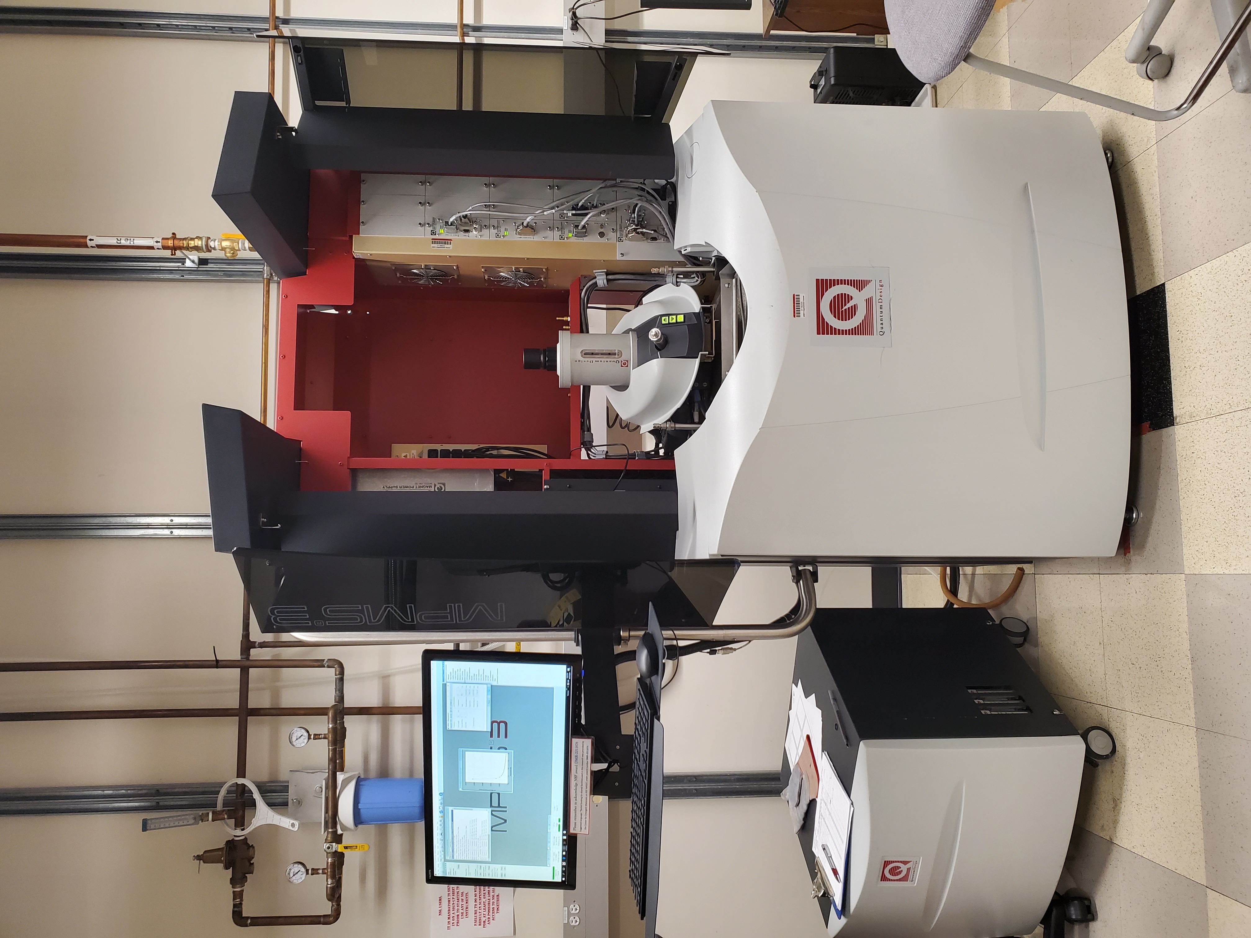
Squid Magnetometer (New SQUID) (Quantum Design MPMS 3)

Located in PRB 1159

  • Broad temperature range of 1.9 K ~ 500 K
  • Magnetic field range ±7T
  • The instrument is fully software automated and easy to use
  • AC, DC magnetic moment sensitivity as low as 1.0×10⁻⁸emu
  • Features: Description From Quantum Design Website

  • SQUID Sensitivity
  • 7 Tesla Magnet with QuickSwitch™ technology
  • Maximum ramp rate: 700 Oe/sec
  • Temperature Range: 1.8 ~ 400 K with Rapid Temp™
  • 300 to 1.8 K in 25 min. (typical)
  • Multiple measurement modes (DC, VSM and AC Susceptibility)
  • Software controls for the temperature and magnetic field readily enable the automation of complex data acquisition procedures
SQUID Magnetometer

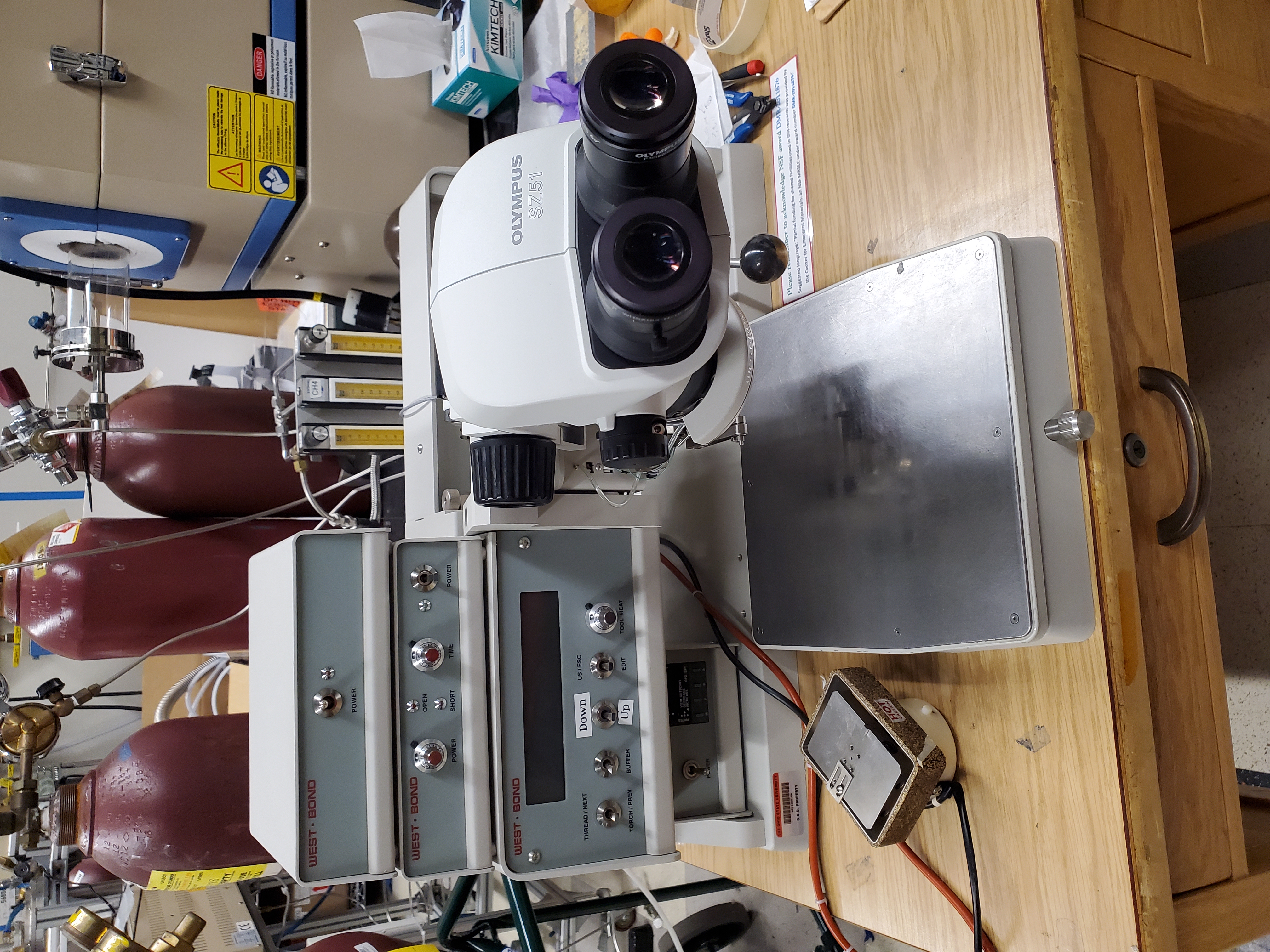
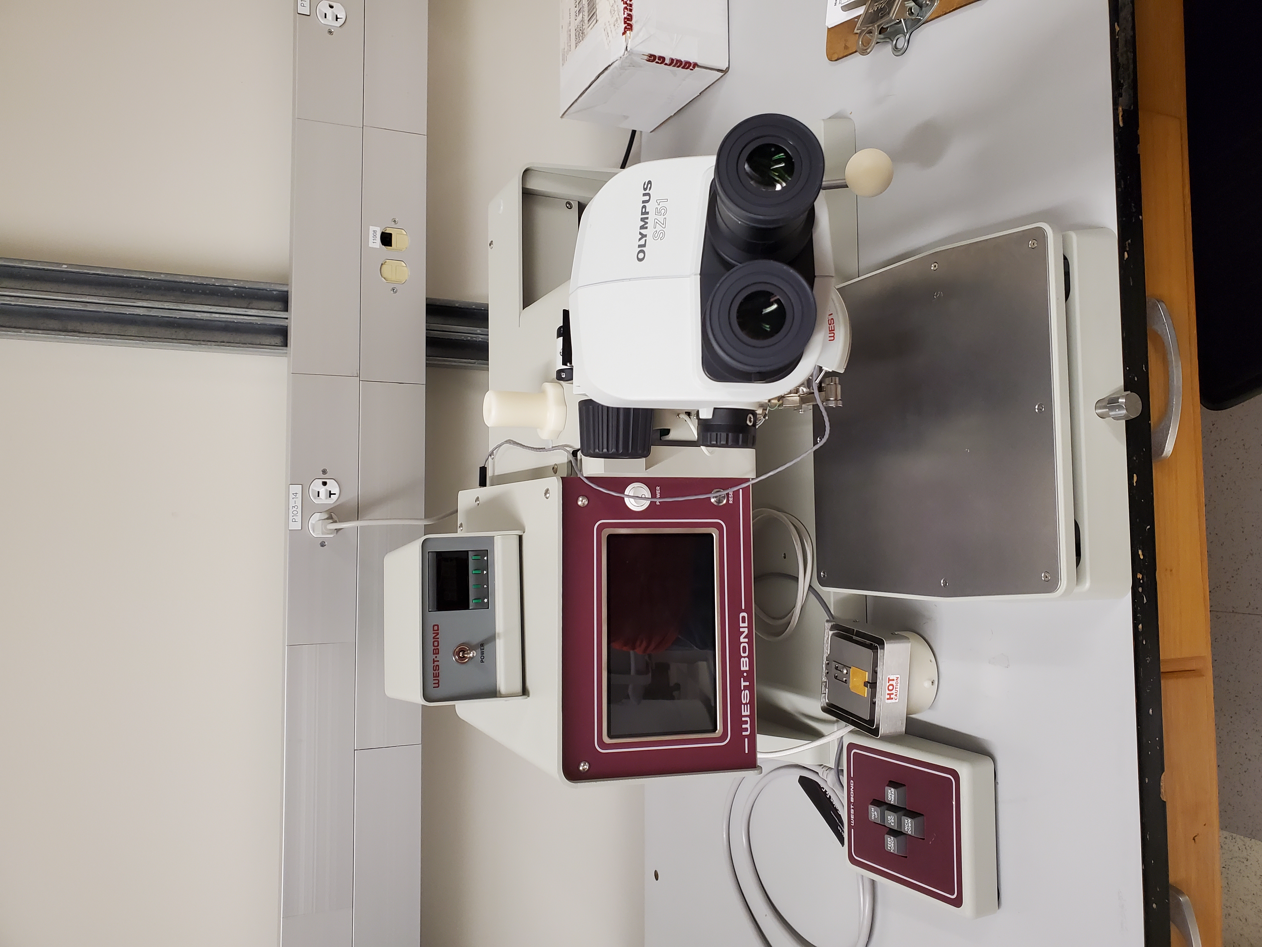
West Bond SZ51 Wire Bonder

Located in PRB 1159

  • a
  • b
  • c
  • d
Wire bonder 1159

West Bond SZ51 Wire Bonder

Located in PRB 1119

  • a
  • b
  • c
  • d
Wire bonder 1119

Bruker D8 Discover High-Resolution Triple Axis X-Ray Diffractometer

Located in PRB 0177

  • Third generation Göbel mirrors providing the highest X-ray flux density - essential for all thin film applications
  • Easy and failsafe operation - tools like the motorized absorber allow fully automatic operation without user intervention
  • High performance optics for optimum resolution
  • X-ray source: Cu Kα1
  • Data processing software includes Leptos and Topaz
Applications:
  • High resolution X-ray Diffraction
  • Texture and Stress Analysis
  • X-ray reflectometry
  • Grazing Incidence Diffraction (GID)
  • Powder Diffraction
X-ray Diffractometer